Section 7.7 · Topic 1 of 10
7.7.1 The microstrip line and why it is not TEM
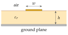
A microstrip line (Figure 7.7.1a) is a conducting strip of width on a dielectric substrate of relative permittivity and height , which covers a conducting ground plane. The strip is thin, , and the line is uniform along .

Why not TEM?
Suppose the wave were TEM, , with the factor . The -component of and the -component of then read, in each region,
wherever the field is not zero. In the air this demands , in the substrate . The field lives in both regions and has one , so a TEM wave is impossible. The true modes are hybrid, with small longitudinal components and (Orfanidis, Section 11.3, shows the same from the boundary conditions at the air–substrate interface).
Quasi-TEM
As long as the substrate is thin compared with the wavelength, , the longitudinal fields stay tiny and the transverse field is, to a very good approximation, the static field of the two conductors. The wave then behaves as a TEM wave in a uniform medium of an effective permittivity , with . This quasi-TEM picture is the basis of all microstrip design.
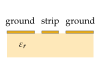
Common substrates are FR-4 glass epoxy (, ), PTFE and hydrocarbon laminates ( to , to ), alumina () and gallium arsenide (). Two relatives are shown in Figure 7.7.1: the stripline, buried between two grounds in a homogeneous dielectric, carries a true TEM wave (like the coaxial line of Section 7.5), and the coplanar waveguide has its grounds on the same face as the strip.